
Samsung is reportedly removing Fan-Out Panel Level Packaging from its next flagship in-house chip, the Exynos 2700, reverting to a more conventional packaging method to reduce manufacturing costs and improve production yield rates ahead of the Galaxy S27 series.
What FOPLP Actually Does — and Why It Is Expensive to Build
Chip packaging is not just an enclosure. It determines how thin a chip stack can be, how efficiently heat escapes the die, and how reliably the chip can be manufactured at scale. In a standard Package-on-Package arrangement — the approach Samsung used on several earlier Exynos chips — a logic die and a memory die sit in a layered stack on a PCB substrate, connected by solder balls. The substrate adds structural rigidity, but it also adds vertical height and introduces an additional thermal barrier between the logic die and the device's cooling system.
Fan-Out Panel Level Packaging takes a different approach. Rather than stacking on a substrate, the logic die is embedded directly within a redistribution layer — a fine-mesh network of copper interconnects formed on a flat panel. This eliminates the bulk substrate, reduces z-height by roughly 20 percent according to the user-supplied structural data underlying this analysis, and improves heat dissipation by shortening the distance between the die and the thermal interface above it. On paper, it is a better design for a high-performance mobile chip running on a dense 2nm process node.
The problem is manufacturing complexity. Forming a reliable redistribution layer at panel scale, with the dimensional tolerances required for a 2nm die, is technically demanding. Yield rates — the percentage of chips that pass quality checks — have historically been variable with advanced packaging at new process nodes, adding unpredictability to per-unit cost. The diagram below shows how the two stack architectures differ and why FOPLP's structural advantages come with a more complex build path.
The Cost-Yield Tradeoff Driving the Exynos 2700 Decision
Samsung's internal calculus, as reported across multiple industry sources, comes down to a straightforward tension: FOPLP delivers better chips but produces them less predictably, and at a higher per-unit cost.
That cost pressure has a specific external driver. Qualcomm's Snapdragon 8 Elite Gen 6 — the competing chip Samsung would need to license for regions where the Exynos 2700 would not be used — is reported to cost OEMs upwards of $240 to $260 per unit. If Samsung can manufacture a 2nm Exynos 2700 with standard or Fan-Out Wafer Level Packaging at a materially lower cost, it preserves the financial rationale for maintaining its dual-track chip strategy. If advanced packaging absorbs too much of that saving, the case for producing the Exynos at all weakens.
The 2nm SF2 node itself adds yield risk independent of packaging. Samsung's sub-3nm nodes have carried below-industry-average yield rates in prior generations, according to reporting on the foundry's production challenges. Layering a novel panel-level packaging process on top of a new process node compounds that risk. Reverting to a packaging method with a longer manufacturing track record may be less about the packaging technology itself and more about controlling the cumulative risk surface on a chip that needs to be ready in volume for a 2027 launch window.
The chart below maps where Standard Packaging and FOPLP each sit on the two axes that define Samsung's decision: production cost and thermal efficiency.
What the Packaging Downgrade Means for Galaxy S27 Performance and Thermals
The practical question for buyers is whether removing FOPLP will result in a chip that throttles under sustained load. That question cannot be answered definitively yet, because no thermal measurements of an Exynos 2700 with standard packaging exist at this stage of development.
What the source reporting does establish is that FOPLP's thermal advantage is specifically relevant in high-performance scenarios — prolonged gaming, extended video encoding, sustained AI inference workloads. These are exactly the use cases where modern flagship chips are most likely to hit thermal limits. Whether Samsung's 2nm process node is efficient enough to compensate for a less optimized heat path, or whether the chip will rely on device-level cooling solutions to close the gap, is not yet confirmed by any sourced technical data.
It is also worth noting that this decision is still reported, not officially confirmed by Samsung. The company has not publicly addressed the Exynos 2700's packaging method or the Galaxy S27's chip configuration. The information comes from industry supply chain reporting, which has tracked Samsung's flagship chip roadmap with reasonable accuracy in prior cycles but does not carry the authority of an official filing or announcement.
What the move does confirm, if the reports hold, is that Samsung is prioritizing production economics and supply chain predictability over maximum technical performance in its in-house chip program. For a division that has faced persistent questions about Exynos competitiveness in recent generations, that is a notable constraint — but it may also be the constraint that keeps the Exynos 2700 viable at all, against a Qualcomm alternative that reportedly costs OEMs significantly more per unit.
Related Stories

OpenHuman: Open-Source Local AI Agent With 118 Integrations
OpenHuman is an early-beta, GNU-licensed desktop agent by tinyhumansai that locally stores context from 118 integrations and routes tasks across multiple LLMs without a cloud dependency.

Scientific Agent Skills: 135 Open-Source AI Research Tools
K-Dense has renamed its open-source repository to Scientific Agent Skills and launched K-Dense BYOK, a desktop co-scientist supporting 40+ models and local-to-cloud scaling via Modal.

Snapdragon 8 Elite Gen 6 Pro Price Leak: What It Costs OEMs
Reports suggest Qualcomm's 2026 flagship chip could cost OEMs up to $290, a sharp rise driven by TSMC N3P process economics, with a broader product tier strategy intended to protect mid-range Android makers.
TanStack npm Supply Chain Attack: How It Happened
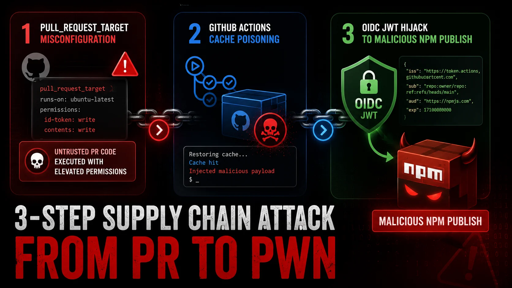
A May 2026 supply chain attack on TanStack npm packages used pull_request_target abuse, GitHub Actions cache poisoning, and OIDC token hijacking to publish malicious packages with valid SLSA provenance.
Comments (0)
Please sign in to join the discussion.
No comments yet.
Be the first to share your perspective on this topic.