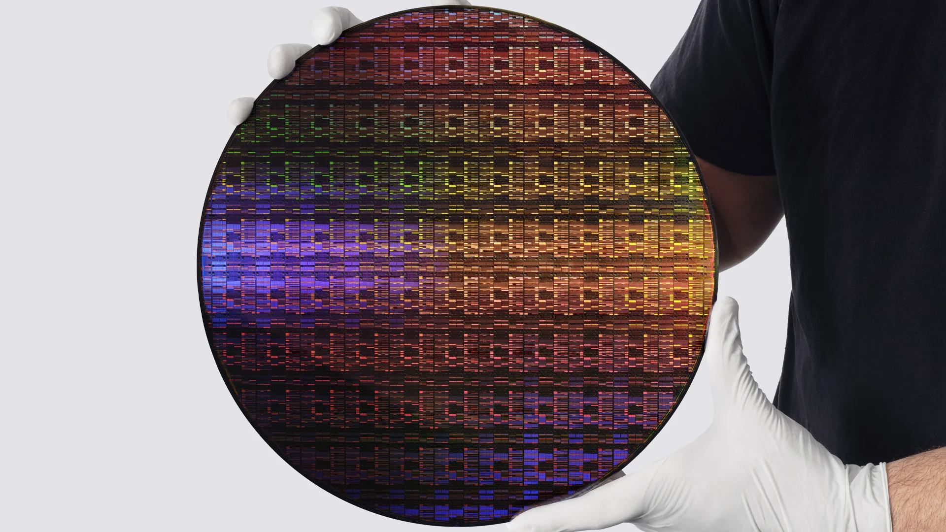
On June 25, 2026, IBM announced what it describes as the world's first sub-1-nanometer chip technology — a 0.7nm node, equivalent to 7 angstroms, where individual transistor features are now measured in single-digit atom widths. The announcement marks a practical boundary in semiconductor physics, not just a generational label change.
Why 7 Angstroms Is Different From Prior Node Shrinks
For most of the past decade, "node" numbers in the semiconductor industry have been marketing shorthand rather than physical measurements. A "5nm" chip does not have features that are literally 5 nanometers wide. The numbers reflect process generations, not geometry. At 7 angstroms, however, the distinction collapses: transistor components are now operating at dimensions where individual atomic layers become meaningful engineering constraints. Quantum tunneling, dopant atom placement, and thermal noise behave differently at this scale than they do even at 2nm or 3nm. That is the engineering context IBM is working in, and it changes what tradeoffs are available.
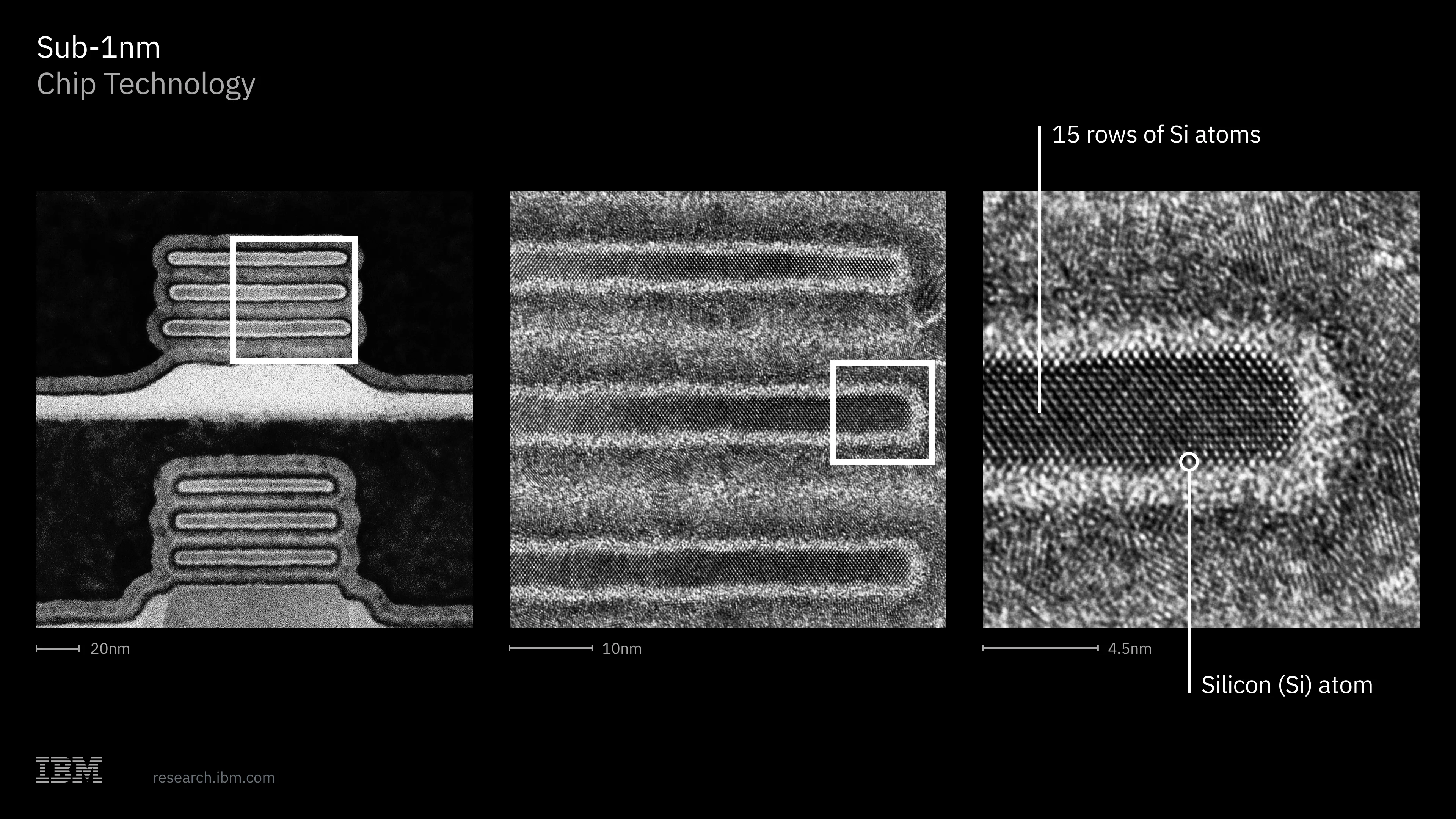
The company's answer is an architecture it calls Nanostack — the first 3D, nanosheet-based transistor design to use vertical stacking and staggered layer arrangement through 3D sequential integration. Standard nanosheet transistors are flat; Nanostack stacks them vertically. Critically, each stacked layer can use a different material combination, which means engineers can tune power and performance characteristics layer by layer rather than applying a single material set across the entire structure. IBM confirmed the architecture has been mechanically and chemically validated through ultra-thin dielectric bonding in CMOS integration, dual-channel engineering, and demonstrated working functional CMOS inverter operation. These are laboratory validation steps, not production metrics.
The four key figures IBM announced — transistor density, projected performance, projected energy efficiency, and SRAM area scaling — are summarized below.
What the Demonstrated Metrics Mean — and What Remains Projected
The transistor density figure — approximately 100 billion transistors on a chip the size of a fingernail — is roughly double what IBM reported for its 2021 2nm node. IBM also demonstrated a 40% reduction in SRAM cell area, which matters directly for AI workloads: generative inference and training pipelines are frequently bottlenecked by memory bandwidth, and denser on-chip SRAM allows more data to remain closer to compute. Both of these are demonstrated results from laboratory fabrication, not estimates.
The performance and efficiency projections are a different category of claim. IBM states Nanostack could deliver up to 50% more performance or up to 70% greater energy efficiency compared to its 2nm node. These are IBM's own projections, compared against IBM's own prior process. No independent benchmarks from third-party chip designers or foundry customers are cited in the announcement. The "or" construction in the performance-vs.-efficiency framing is also significant from a design standpoint: these gains represent ends of a tradeoff spectrum, not simultaneous outcomes. A chip tuned for maximum performance will not also capture the maximum efficiency gain.
The chart below shows what IBM projects these gains look like relative to the 2nm baseline.
The Fabrication Ecosystem and the 5-Year Path to Commercial Production
IBM did not build this architecture in isolation. The research was conducted at its Albany, New York facility using ASML's High Numerical Aperture Extreme Ultraviolet (High NA EUV) lithography tools — the same class of equipment that TSMC and Intel are deploying in their leading-edge fabs. Alongside ASML, IBM worked with Lam Research, Tokyo Electron (TEL), and SCREEN Semiconductor Solutions on process integration. The presence of these partners is relevant: it indicates the architecture has been stress-tested against production-grade tooling rather than bespoke research equipment.
IBM projects that the earliest adoption path and a route to commercial production will emerge within five years, placing the realistic commercialization window around 2031. IBM also states that Nanostack extends the semiconductor scaling roadmap by at least a decade. That is an ambitious projection for technology that is still at the laboratory demonstration stage. The gap between a working CMOS inverter — which confirms the architecture's basic switching logic is functional — and a full production chip with billions of transistors operating reliably at yield is substantial. No foundry partner announcements, licensing agreements, or manufacturing transfer agreements are mentioned in the announcement.

The 0.7nm node also sits alongside a separate strategic move IBM announced recently: the creation of Anderon, described as the world's first pure-play quantum foundry for manufacturing quantum wafers in the United States. The two programs are distinct — classical silicon scaling and quantum fabrication are separate manufacturing disciplines — but together they signal IBM's positioning across multiple long-horizon compute bets.
The timeline below maps the node progression from IBM's 2nm demonstration through the Nanostack announcement and the projected commercialization window.
The Nanostack announcement represents a genuine laboratory milestone: a working architecture that operates below 1nm, validated with functional switching logic and demonstrated SRAM scaling at production-relevant tooling. The more significant constraint, for engineers and investors evaluating the semiconductor roadmap, is the gap between that milestone and a chip that a customer can order. IBM has not named a manufacturing partner, a licensing path, or a volume production target. The five-year estimate to commercial adoption, measured against the industry's history of sliding timelines at leading-edge nodes, should be treated as an optimistic lower bound rather than a schedule.

Qwen 3.6 27B Hits GPT-5-Era Scores on a MacBook
Reviewer Piotr Migdał's local tests show Qwen 3.6 27B trading speed for code quality against the 35B A3B variant, with full llama.cpp and benchmark data.

How SQLite Databases Actually Get Corrupted
A breakdown of how SQLite databases get corrupted despite the engine's built-in crash resistance, drawn from SQLite's official corruption documentation.
Samsung, SK Hynix, Micron Sued Over DRAM Price-Fixing
Fourteen consumers and three small businesses sue Samsung, SK hynix and Micron, alleging coordinated DRAM supply cuts behind chipflation and a 700% price climb.

China's 360 Security Claims Mythos Rival After Export Ban
Qihoo 360 CEO Zhou Hongyi unveiled Tulongfeng at ISC.AI 2026, positioning it as China's answer to Anthropic's Mythos. The claim rests on an agentic workaround, not a benchmark result — and remains unverified by independent parties.
Comments (0)
Please sign in to join the discussion.
No comments yet.
Be the first to share your perspective on this topic.