
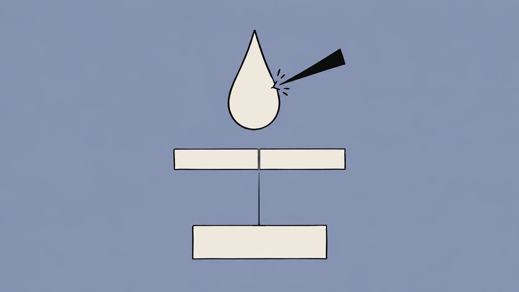
ASML is the world's only manufacturer of extreme ultraviolet (EUV) lithography systems, according to its annual report filed with the SEC, and every one of those machines makes its light the same way: a pulsed laser strikes microscopic tin droplets inside a vacuum chamber. The plasma that results emits 13.5 nm radiation, which the scanner uses to expose the finest layers of advanced logic and memory chips. Two numbers decide how fast and how finely a system can print: the power of that light source and the numerical aperture (NA) of the optics.
Laser-produced plasma turns molten tin into 13.5 nm light
In a laser-produced plasma (LPP) source, molten tin droplets are fired through a vacuum chamber, tracked individually and vaporized by a high-power pulsed laser as often as 50,000 times per second. A large mirror collects the 13.5 nm light and directs it into the scanner, where it passes through a photomask and is projected onto a silicon wafer.
The main CO2 laser pulse is preceded by a smaller one. A pre-pulse reshapes the tin droplet into a target with a better shape and density, which raises the share of laser energy converted into EUV radiation. That conversion efficiency is one of the main reasons the approach reached production power levels at all.
The reason chipmakers accept this complexity is process simplification. ASML's filing says EUV lets customers shift from multi-patterning to single patterning, a method that needs only one exposure per layer, where deep ultraviolet (DUV) immersion systems need several.
Source power rose from 75 W to a 1,000 W proof of concept
The chart below arranges five reported source-power milestones from different years, to show the direction and scale of the climb.
The figures are not strictly like for like. The 2009 value is full-die exposure power from the first integrated source shipment, the 2015-16 value is dose-controlled power at the intermediate focus, and the 250 W value comes from field-operating sources reported to SPIE. The two latest values are ASML's own: its current highest-power industrial source on High NA scanners is 600 W, and a validated proof of concept reaches 1,000 W.
That proof of concept combines three changes: higher-power laser pulses, a tin droplet rate raised from 60 to 100 kilohertz, and droplet preshaping before the main hit. The droplet rate rises by a factor of 1.67, and so does the power (1,000 W over 600 W). The coincidence is tempting to read as droplet rate alone explaining the gain, but the reported figures do not separate the three contributions, so that attribution is unsupported. For comparison, the 2009 source fired at up to 50 kHz, which means the droplet rate has doubled over the technology's history while power grew more than thirteenfold.
Raising numerical aperture to 0.55 shrinks the printable feature to 8 nm
Source power determines how quickly a wafer can be exposed. Numerical aperture determines how small a feature the optics can resolve. ASML's TWINSCAN NXE platform uses 0.33 NA, while the TWINSCAN EXE platform uses 0.55 NA, with a critical dimension of 8 nm. ASML states that the EXE:5200B prints features 1.7 times smaller in a single exposure and reaches transistor densities 2.9 times higher than NXE systems. The two claims agree arithmetically, since 1.7 squared is 2.89.
| System | NA | Resolution | Throughput | Overlay |
|---|---|---|---|---|
| NXE:3600D | 0.33 | about 13 nm | 160 wph | 1.1 nm |
| NXE:3800E | 0.33 | about 13 nm | up to 220 wph | 0.9 nm |
| EXE:5200B | 0.55 | 8 nm | 175 wph at 50 mJ/cm² | 0.7 nm (Intel-reported) |
Sources: ASML's FY2024 filing for NXE figures, the EXE:5200B product page and Intel's installation announcement as reported for EXE figures. The 13 nm low-NA resolution is cited in the same Intel coverage.
The timeline for volume use has moved. ASML's FY2024 filing expected the EXE platform to support high-volume manufacturing in 2026, while the FY2025 filing says 2027. ASML's chief executive is reportedly looking at mass production in 2027 to 2028, and the same coverage says a Hyper NA step is under research for the following decade.
The 220 and 175 wafer-per-hour figures describe different operating points
A glance at the table suggests the High NA tool is slower than the NXE:3800E. That reading overlooks exposure dose. ASML quotes the EXE:5200B's 175 wafers per hour at 50 mJ/cm², and a secondary technical summary reports the NXE:3800E's 220 wafers per hour at 30 mJ/cm². None of the cited sources places both platforms at a single dose, so the two throughput numbers cannot be ranked against each other.
Within the High NA line the comparison is cleaner. ASML says the EXE:5200B delivers 60% higher productivity than the EXE:5000, credited to an improved light source delivering more power at the wafer. This suggests that source power, the subject of the chart above, is the main lever on High NA throughput, so the 600 W to 1,000 W step bears directly on the economics of the 8 nm tools.
Forty-eight EUV systems brought in €11.6 billion, roughly €242 million each
ASML's results call reported EUV system sales of €11.6 billion from 48 systems, including High NA, which was 39% higher than the prior year. Dividing one by the other gives about €242 million of recognized revenue per system. That is an average of mixed 0.33 NA and 0.55 NA sales, and revenue recognition timing means it is not a list price for any one model.
Demand visibility is also sourced: of a €38.8 billion year-end backlog, €25.5 billion was EUV, close to 66%. Logic accounted for 70% of net system sales in the fourth quarter and memory for 30%.
Alternative EUV sources need an uptime or cost edge, since power is no longer the gap
According to Bits&Chips, at least three companies, Substrate, Tau Systems and XLight, are pursuing alternative EUV source technology. With the Bits&Chips report concluding that source power will not limit throughput once the 1,000 W source is industrialized, those challengers would have to show an advantage in uptime, power consumption or overall cost. No cited source reports such a result yet, and the other open question is the date High NA tools reach volume production, which ASML now places in 2027.
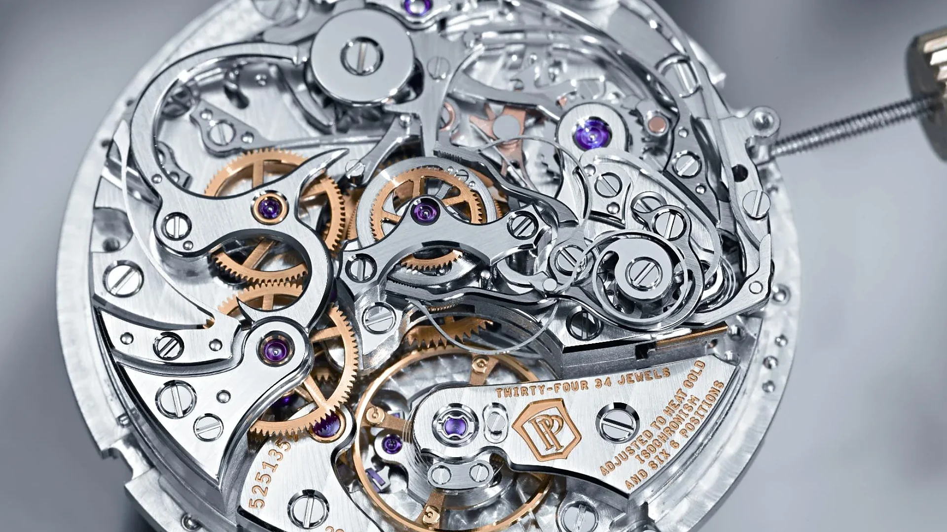
How Quartz Watches Actually Work, and Why Mechanical Watches Still Sell
A quartz crystal oscillating at 32,768 Hz, divided into one pulse a second, keeps quartz watches accurate to seconds a month, mechanical still costs more.

IonQ's Revenue Jumped 287% in Q2 2026, but Its Stock Is Still 47% Below Its High
IonQ's Q2 2026 revenue rose 287% to $80.1 million and guidance climbed to $280-$290 million, yet IONQ shares still trade 47% below their October peak.
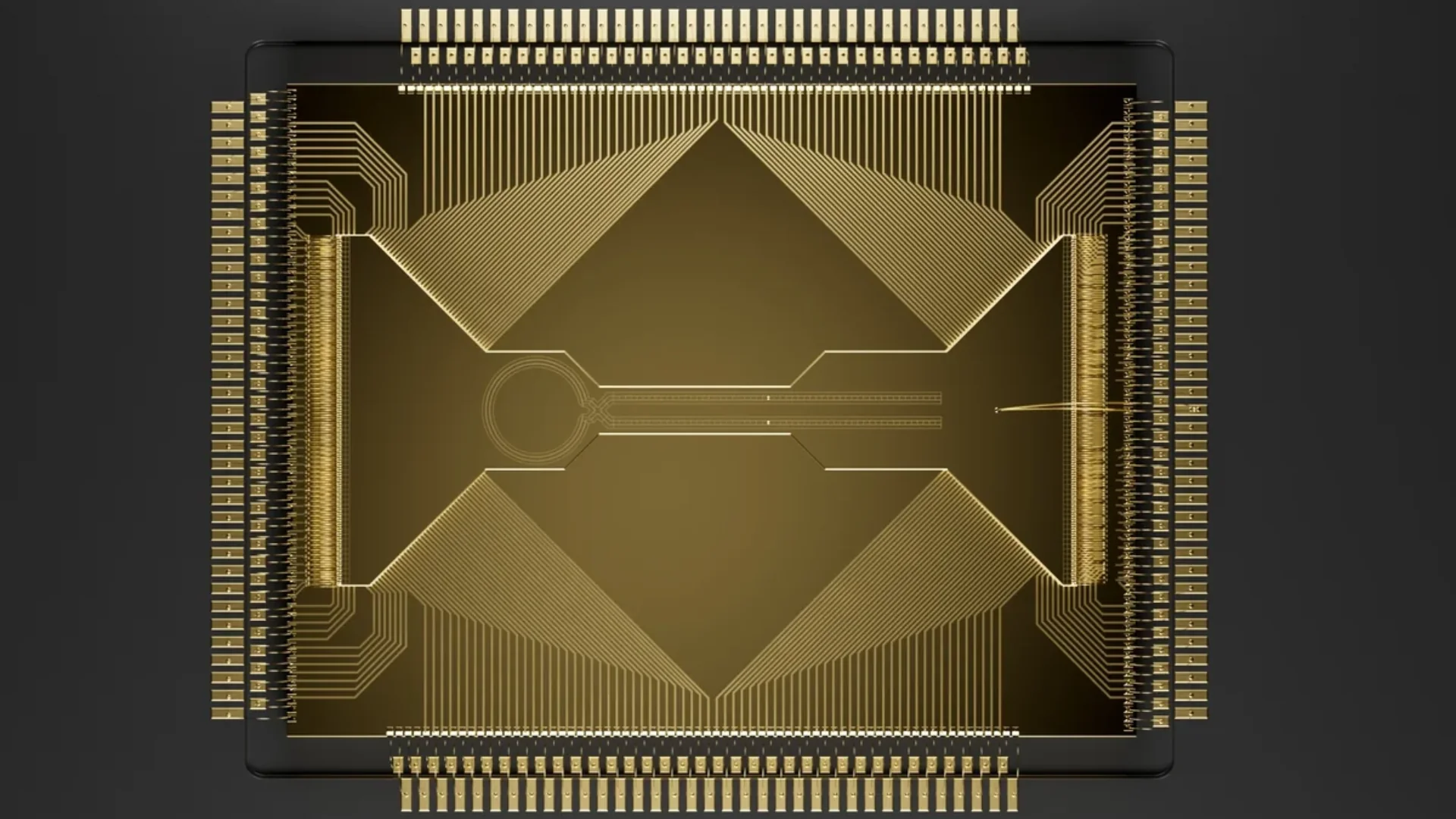
Quantum Computing's Shift From Research to Infrastructure
Three 2026 developments — Quantinuum's Helios, IBM's Anderon foundry, and Illinois's quantum park — mark a shift from qubit-count races to manufacturing and workforce infrastructure.
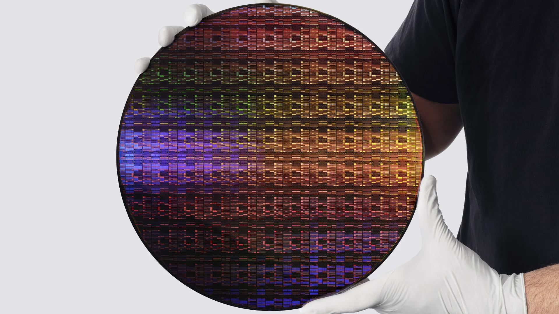
IBM 0.7nm Chip: What Nanostack Changes for AI Hardware
IBM's Nanostack architecture stacks transistors in 3D at 0.7nm, doubling density over its 2nm node, with up to 50% performance gains or 70% energy efficiency gains and a 5-year path to commercial production.
Comments (0)
Please sign in to join the discussion.
No comments yet.
Be the first to share your perspective on this topic.